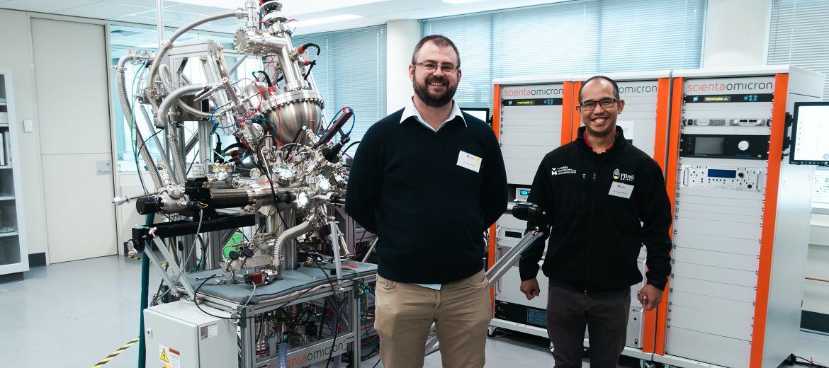
By Benjamin Chambers and Tanglaw Roman – Flinders University, Flinders Microscopy and Microanalysis
Photoemission electron microscopy is suitable for measuring the chemical and physical properties of conductive samples in an ultra-high vacuum (UHV) environment. Photoemission electrons generated by monochromatic UV light (21.2 / 40.8 eV) can be focused and detected to construct an image of the surface. PEEM images have contrast created by variations in the surface morphology, probability of photoemission, and work function across the surface. The PEEM energy-filtered images have a lateral resolution of <50 nm and fields of view ranging from 10-160 µm.
In addition to imaging the surface in real space, the electrons can be focused onto the detector in a way to map the momentum of the photoemission electrons; known as momentum microscopy (MM). These momentum images map the variation in electron ejection angles, providing a form of angle-resolved photoelectron spectroscopy (ARPES). In contrast to traditional ARPES, the sample angle is fixed and all angles are measured simultaneously. Small areas (~10 µm) can be selected for µARPES studies. The µARPES is a powerful technique for investigating the electronic band structure of materials.
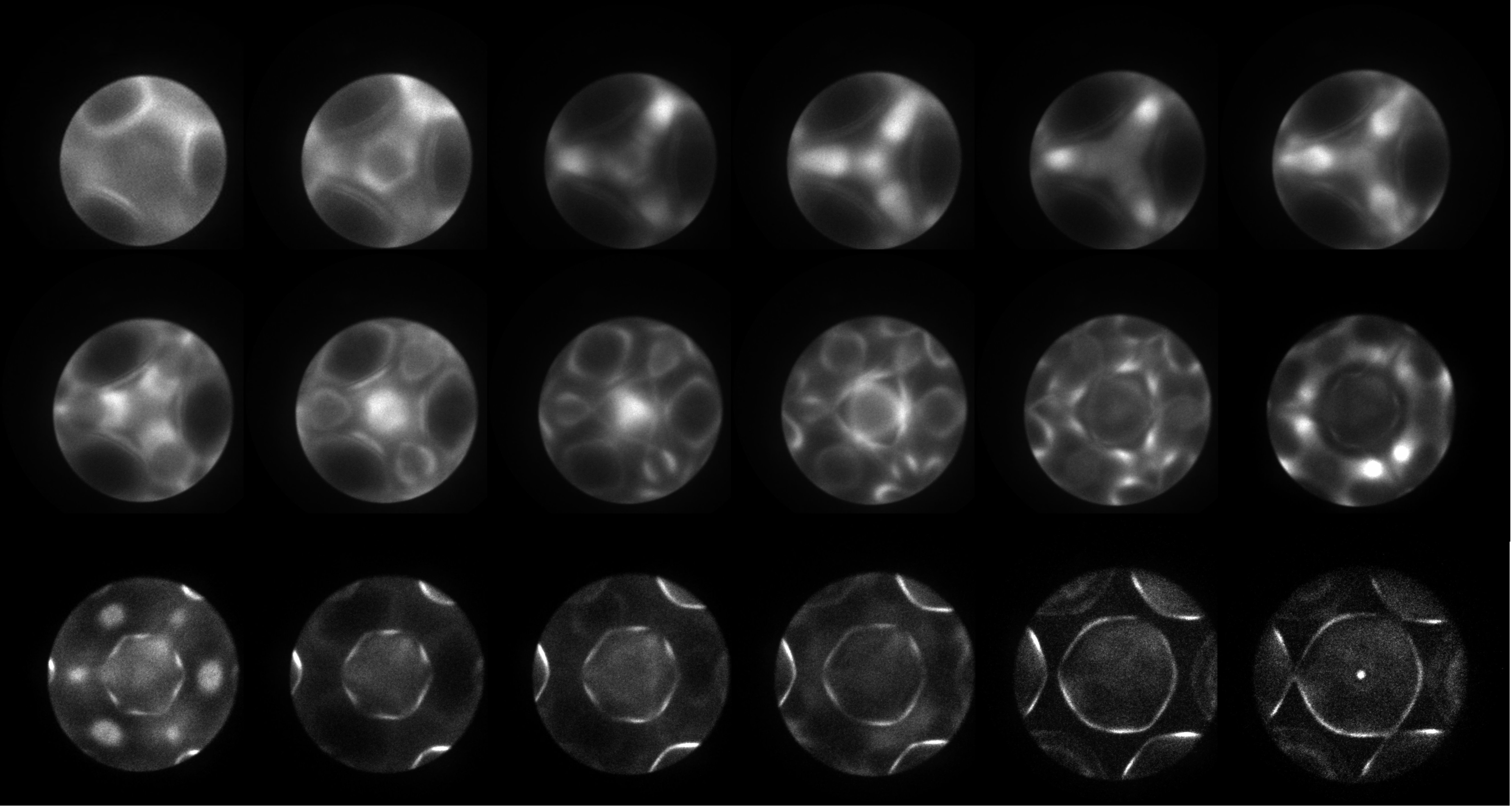
Full wavevector ARPES images: Ag (111) FoV 5Å-1
Using a monochromatic X-ray source (Al Kα 1486 eV) the NanoESCA III is also capable of chemical analysis by imaging photoemission electrons (XPEEM) and small spot (~500 nm – 200 µm) X-ray photoelectron spectroscopy (XPS).
The NanoESCA III preparation chamber is equipped with a suite of tools:
The NanoESCA III enables the direct correlation between electron band-structure of advanced materials with device function. This is essential for understanding electron transport in materials including topological insulators and transistors for quantum computing, nanomaterials for energy-storage devices and catalysis, and minerals for geoscience.
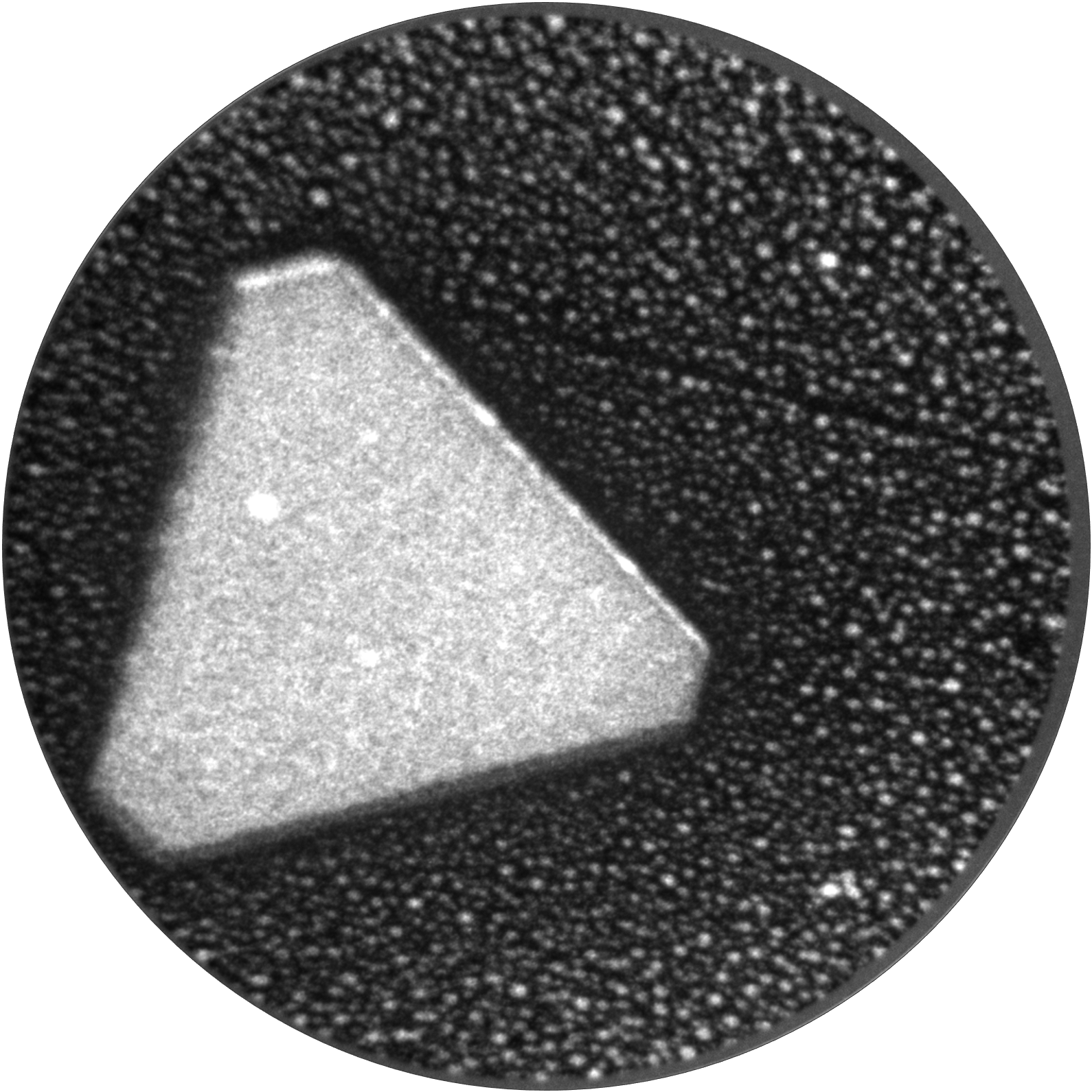
Real space PEEM image: 20µm FoV, E-Ef: 4.5eV, gold on silicon
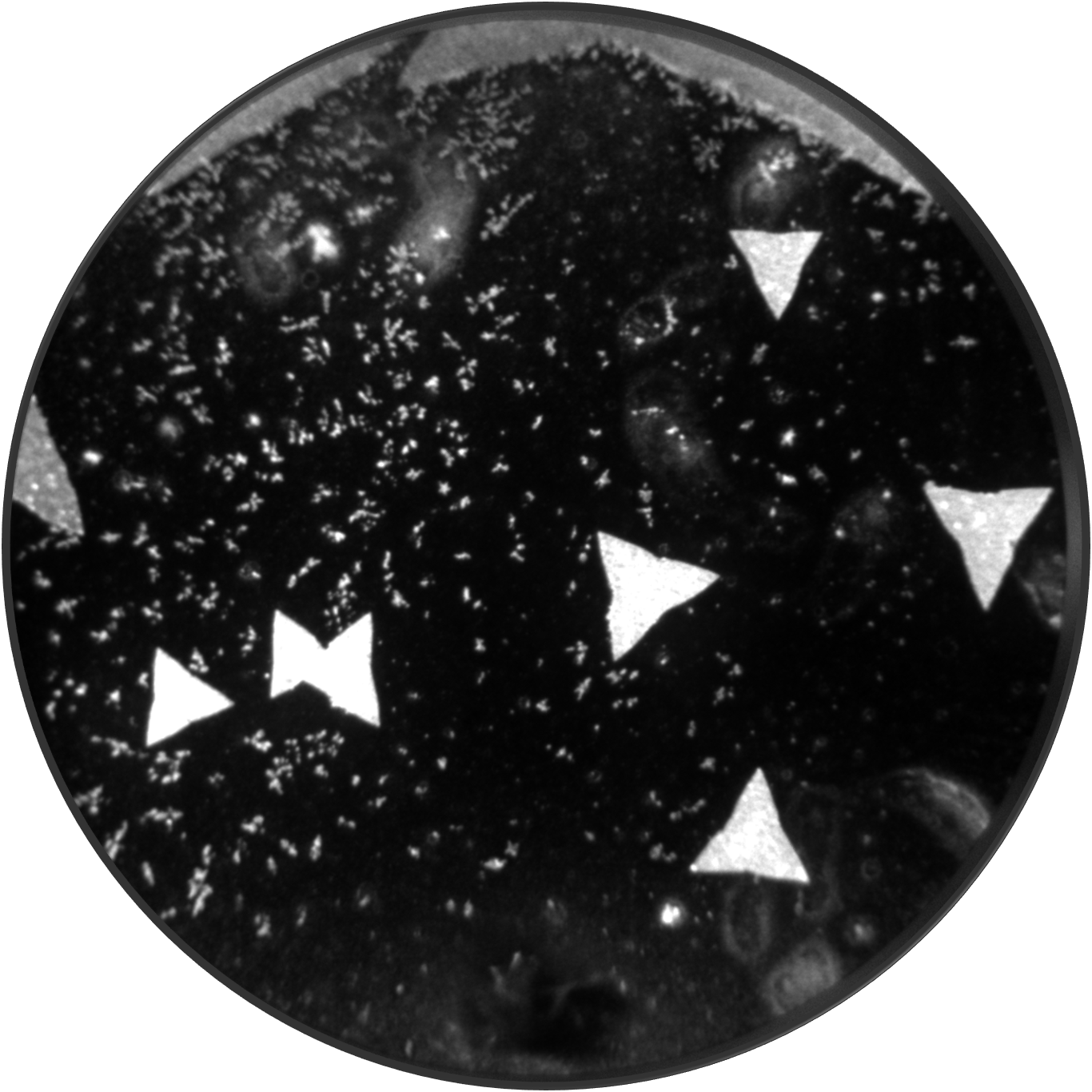
Real space PEEM image: 76µm FoV, E-Ef: 4.825eV, CVD grown MoS2 on silicon
March 20, 2024