Silicon, which has been used since the beginning of modern computing, is currently etched into layers of interconnecting silicon nanowires processed so that electrons only need to travel approximately three nanometres to carry signals around the chip. As this is the thickness of only a few atoms, it leaves hardly any room to manoeuvre: silicon chips are approaching their minimum possible size.
To overcome this problem, a new material called indium arsenide (InAs) is being explored. Even though indium and arsenic atoms are larger than silicon atoms, electrons can flow faster through them than through silicon.
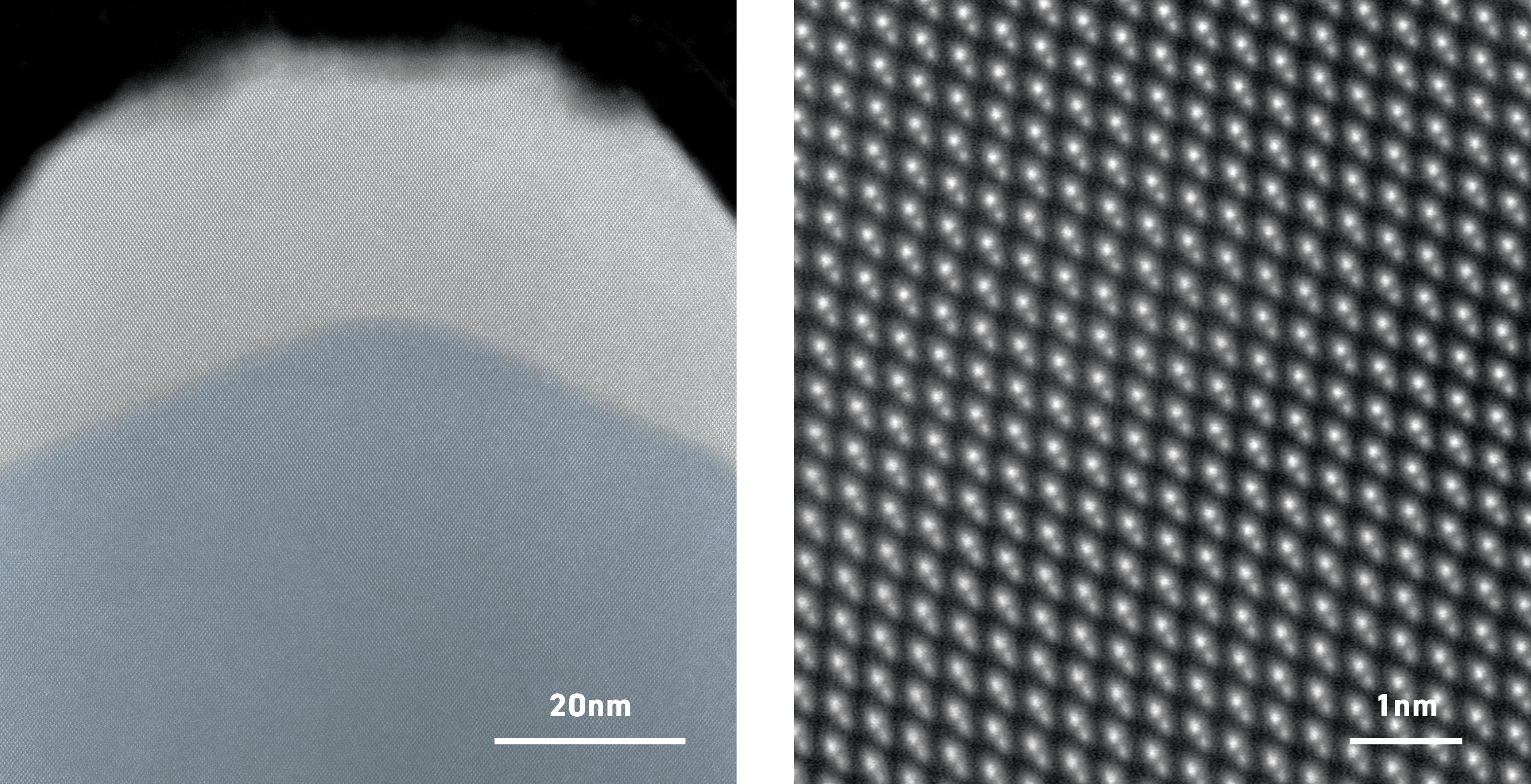
Research collaborators in Denmark have grown nanowires made of InAs. These need to be grown at high temperatures around an indium gallium arsenide (InGaAs) core (blue in image below). However, at these high temperatures, indium and gallium diffuse easily. When the gallium diffuses from the core into the outer InAs layer, it compromises the purity of that layer, reducing its electron-carrying capacity. Microsoft wanted to know how they can visualise the extent of that diffusion.

Scanning transmission electron micrographs of the atomic structure of the nanowire. Blue shows the core of the wire.
By using atom probe tomography and atomic-resolution scanning transmission electron microscopy at Microscopy Australia’s University of Sydney facility, the researchers were able to accurately measure how much diffusion had occurred during nanowire growth to help inform the design of these nanowires into the future.
J. Qu et al., Applied Materials & Interfaces 2022
DOI: 10.1021/acsami.2c09594
Crosssection of the top of a nanowire made of indium arsenide (grey in image). These need to be grown at high temperatures around an indium gallium arsenide core (blue in image)
September 28, 2022