They can be efficiently produced via a bottom-up growth system known as the vapour-liquid-solid mechanism. Despite considerable investigations into the growth and evolution of these nanowires, the presence of specific atoms and impurities cannot be discerned at the atomic scale using most current techniques.
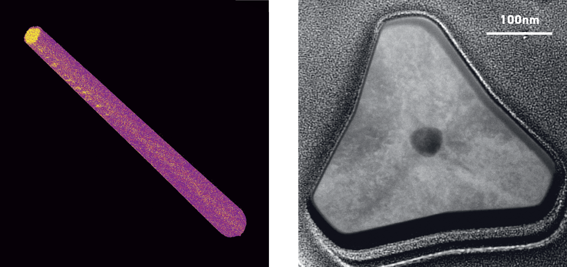
Recent research by Jiangtao Qu, A/Prof. Rongkun Zheng and colleagues from the University of Sydney (USyd), together with collaborating institutions, mapped the number and 3D position of different types of atoms within a single indium-gallium-arsenic (InGaAs) nanowire, just 50nm in diameter. This was made possible by flagship atom probe tomography (APT) at Microscopy Australia’s USyd facility. Atom probes are the only types of instrument that can provide this kind of information.

Left: APT image of a nanowire showing the gallium atoms in yellow and the indium atoms in purple. Right: TEM image of a nanowire cross-section showing the core-shell structure.
The team also prepared tiny specimens with a focused ion beam that were analysed in the transmission electron microscope. This data formed a basis for the reconstruction of APT data.
Tomography revealed that the core and shell of these nanowires exhibited directional growth and that atoms migrated between the core and the shell of the structure. The team used this insight to propose a new model that explained these atomic-scale 3D observations.
Such unprecedented 3D insights into nanowire structure and shape enable deeper understanding of the relationship between nanowire growth habits, their atomic structure and how these characteristics influence their semiconducting properties. This will help facilitate the development of nanowires for increasingly targeted applications.
APT image of a nanowire showing the gallium atoms in yellow and the indium atoms in purple.
July 25, 2017