Many of these TEMs have aberration correction and a number have specialised holders that enable researchers to watch and record atomic arrangements change before their eyes as their samples are stretched, squashed, twisted, heated or cooled. Holders can house small areas of gases or liquids, enabling direct observations of electrochemical processes.
To help highlight what we have and what they can do, here are some of the atomic resolution TEMs in our facilities around Australia and snippets of projects enabled by them.
This is a highly flexible and stable, ultra-high-resolution TEM enabling chemical and structural investigation of complex materials at the atomic level. It incorporates highest brightness X-FEG electron source, 80kV-200kV accelerating voltage, aberration correction on the probe forming lens (DCOR), high precision, Piezo driven specimen stage, tomography capability, SuperX EDS detector technology and Gatan Quantum GIF 965 EEL spectrometer.
Atomic-resolution scanning TEM reveals a disruption in the regular arrangement of atoms in a small piece of the mineral tungsten trioxide, from the Zijinshan copper-gold deposit in China. Tungsten trioxide is a well-known semiconductor with applications in materials science but has not been observed in nature until now.
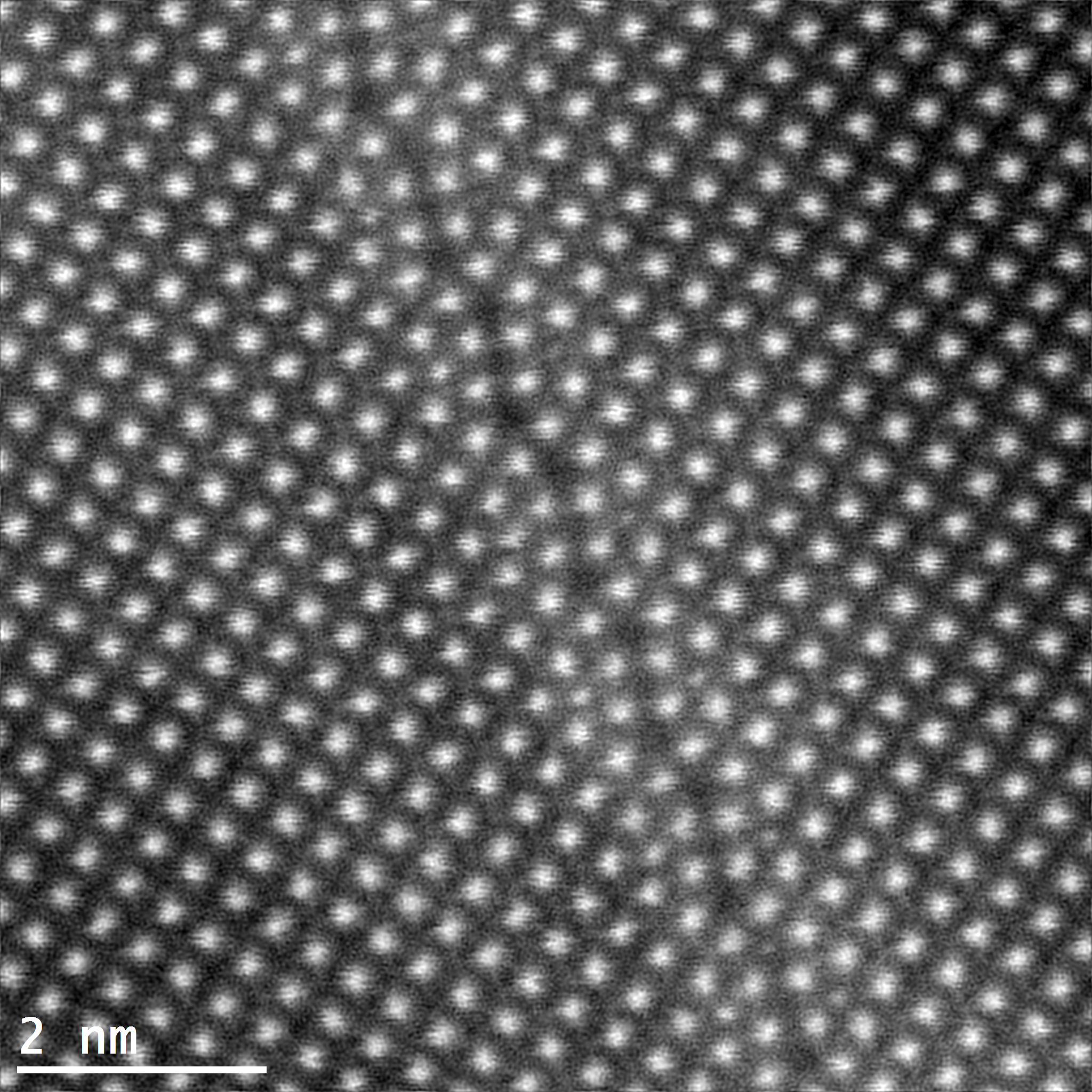
Image captured by Ashley Slattery.
This enables combined high-spectral EELS (<150meV @ 300kV) and spatial resolution of <0.06nm due to its combination of monochromator, XFEG, Quantum 965 energy filter, and DCOR+ probe corrector, with the ability to record ultra-high-count EDS maps with the ChemiSTEM detector system in parallel. An additional materials science TEM is being purchased and will be operational later this year.
Nanoscale cluster of zinc, magnesium and copper in an advanced experimental aluminium alloy – part of a project engineering stronger aluminium alloys at the atomic scale conducted by Li Liu, Keita Nomoto, and Simon Ringer.
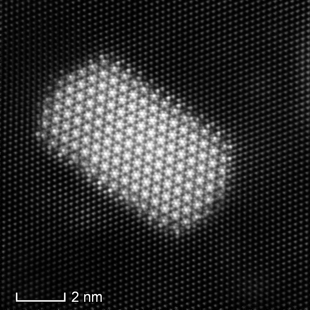
Image by Keita Nomoto
This is a Shottky field emission transmission electron microscope fitted with spherical aberration correctors on the probe and image-forming lens systems. This instrument is capable of imaging atomic structures with a resolution of less than 0.1nm. At the same time, it can acquire chemical information selectively from just one or two atomic columns. The microscope configuration includes electron tomography for 3D imaging of structures and an energy imaging filter for composition and bonding measurements.
Discovery of an intriguing ‘zebra’ structure composed of alternating bilayers of aluminium and silver at the atomic scale. This new phase not only adds a new member to the aluminium-silver system but demonstrates how we can manipulate the clustering behaviour of atoms in alloys. These alloys are studied in order to design better high-strength and lightweight alloys for use in the aerospace industry.

Image captured by Zezhong Zhang.
This is a cold field emission gun (FEG) scanning transmission electron microscope (S/TEM) that operates at 200 kV (with an option of operating at 80 kV). The high brightness and coherence of the cold FEG mean that this microscope is ideally suited for analytical microscopy of materials. The F200 has a lattice resolution of 0.16 nm in ADF STEM mode and 0.1 nm in TEM mode at 200 kV. Facilities available include: a windowless 100 mm2 silicon drift X-ray detector for efficient EDS spectra and elemental mapping at resolution of approximately 0.5 nm; a high tilt holder and TEMography software for acquisition of high angle tilt series in TEM, STEM or EDS imaging modes.
Atomic resolution imaging of platinum–tin nanoparticles to optimise the structure of electrocatalysts. The level of ordering can be controlled by thermal treatment and is measured directly from scanning TEM images. Lower levels of ordering make for more active electrocatalysts but more ordered nanoparticles are more stable.
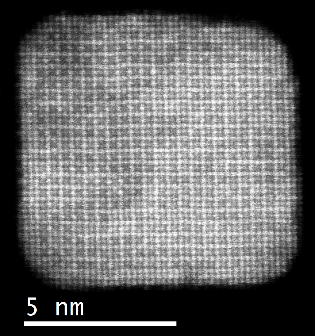
Image captured by Hsiang-Sheng Chen.
A cold field emission transmission electron microscope is fitted with a spherical aberration corrector on the probe-forming lens systems. The HF5000 is capable of imaging atomic structures with a resolution of less than 100pm. It can acquire atomic chemical information using energy dispersive X-ray spectrometry (chemical information) and electron energy-loss spectroscopy (chemical and bonding information). The microscope provides electron tomography for 3D imaging of structures.
Bandgap engineering: this 15nm-diameter hexagonal GaAs nanowire has a gold tip and could be used for tuning LED devices. This study is helping to understand the structure of the doped GaAs nanowires and how strain defects effect the optical properties. These devices are useful because they are compatible with current silicon technology.
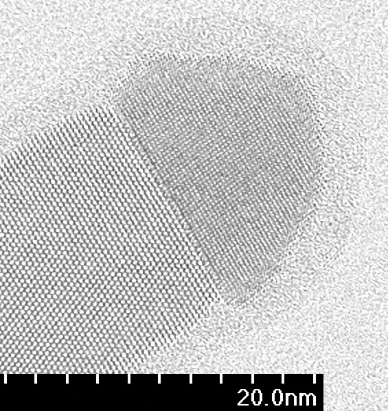
Image captured by Graeme Auchterlonie.
Coloured TEM micrograph taken by Zezhong Zhang, read more about it below.
April 14, 2020